FDS CMR Test
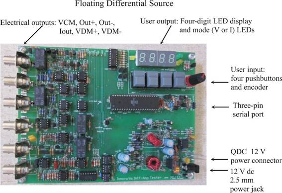
The Innovatia Floating Differential Source (FDS) prototype is a 6 × 8 inch single-board test instrument, shown below.
|
|
FDS CMR Test |
It is a specialized multi-source-measure unit (SMU) designed for testing differential amplifiers and high-side current sensing circuits.
Grounded (common-mode) voltage source with +35 V to –35 V range and 100 mA maximum output current;
Floating (differential-mode) voltage source stacked on the grounded source, with a ±10 V, 100 mA output;
Grounded current sink of up to 100 mA with a voltage range of 5 V to 35 V;
DVM with four-digit or ±10,000 count full-scale display resolution and ±12,500 count internal resolution;
Front panel on board: 4 LED 7-segment digits and polarity sign; voltage-mode and current-mode LEDs;
Serial port: RS-232 communications as alternative command interface to front-panel;
Power supply: 10-output switching converter, powered from 12 V dc, 1 A.
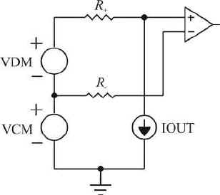
The floating source has BNC outputs VDM+ and VDM–. It is not isolated from the grounded source because VDM– is connected to VCM. It provides a differential voltage that is added to the common-mode voltage of the grounded source. However, it can be used independent of the grounded source as input to circuits isolated from the ground of the grounded source.
The grounded current source sinks current from the IOUT BNC connector and from OUT– in current mode. The OUT+ and OUT– outputs have two configurations: voltage mode (V) and current mode (I), as shown below.
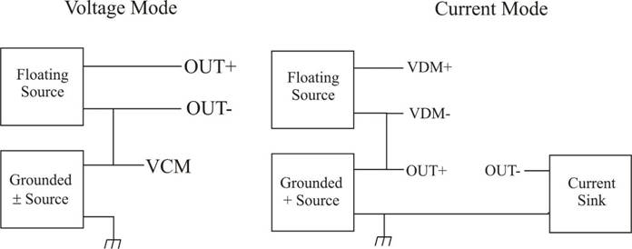
In voltage mode, the floating and grounded sources are stacked in series, as shown. This configuration is useful in testing voltage-input loads such as differential-amplifier common-mode (CM) range, CM rejection, and CM and DM gains and offset, and for determining the calibration parameters for amplifiers in μC-based systems.
In current mode, the current sink is connected to OUT– so that current can flow through a current-driven load from the grounded source. In this mode, the grounded source outputs only a positive voltage as a common-mode or high-side voltage. This mode is useful for testing current-input amplifiers such as high-side current sensors or as input to current-measurement channels of a data-acquisition system. The common-mode voltage allows testing of the current-amplifier input impedance to ground by varying the common-mode voltage. The current sink provides for determination of gain and offset of the current-input amplifier, and determination of calibration parameters of current-input loads.
X dBV º 20·log10(X)
fs: full-scale; zs: zero-scale
Output ±fs voltage range: ±35 V
Output ±zs voltage range: ±0.2 V
Output voltage resolution ≤ 10 mV
Output voltage inaccuracy ≤ 250 ppm = 0.025 %
Output current magnitude ≤ 100 mA
Output impedance, typical: 200 μΩ || 150 μH
Amplifier closed-loop bandwidth, typical = 6.4 kHz
Amplifier closed-loop voltage gain, typical = 8.8433
DM Source Rejection = ΔVCM/ΔVDM » –80 dBV
Noise, rms, 10 kHz bandwidth ≤ 10 mV
Output ±fs voltage range: ±10 V
Output voltage resolution ≤ 2 mV
Output voltage inaccuracy ≤ 250 ppm = 0.025 %
Output current magnitude ≤ 100 mA
Output impedance, typical: 1 mΩ || 1.5 μH
Amplifier closed-loop bandwidth, typical = 6 kHz
CM Source Rejection = ΔVCM/ΔVDM » –80 dBV
Noise, rms, 10 kHz bandwidth ≤ 5 mV
Output current polarity: positive (current sink)
Output fs current range: 100 mA
Output voltage range (compliance): +5 V to +35 V
Output current resolution = 10 μA
Output current inaccuracy ≤ 250 ppm = 0.025 %
Output impedance, typical: 5 MΩ || 15 pF
CM Source Rejection = ΔIOUT/ΔVCM » 1/(5 MΩ)
Noise, rms, 10 kHz bandwidth ≤ 25 μA
Input ±fs measurement range: ±4 V
Overrange » ±25 %
Inaccuracy ≤ 250 ppm = 0.025 %
Resolution = 4 decades (4 digit display) or 12,500 counts
Precision: repeatable to ±1 count in 4 decades
VCM source display resolution = 10 mV
VDM source display resolution = 1 mV
IOUT source display resolution = 10 μA
Display type: 7 segment + r.h. decimal-point LED with negative polarity sign LED; 2 LEDs to indicate V or I mode
Voltage mode: OUT+ connected to VDM+ output; OUT– connected to VCM+ output. DM source is in series with CM source and the CM source negative output terminal is grounded.
RS-232-compatible, with three pins used: ground (GND), transmit out (TXD), receive in (RXD); 0.1 inch spaced square pins on edge of circuit-board; solders without cable to pins 1 - 3 of 9-pin RS-232 connector.
Format (factory default): 19.6 kbaud, 8 bits, no parity, 1 stop bit.
Baud rate can be changed by serial-port command, stored in nonvolatile read-only memory (NVROM).
Input power: 12 V static (dc) ±20 %, 1 A
Input power connectors: 2.5 mm power jack, inner conductor positive; 0.25 inch QDC connectors
Power port emitted noise voltage ≤ 100 mV, 10 MHz
Power port emitted noise current ≤ 10 mA, 10 MHz
Ambient operating temperature range: 20 °C ±15 °C (41 °F ,95 °F)
Ambient specified temperature range: 20 °C ±5 °C (59 °F, 77 °F)
Humidity ≤ 85 %, noncondensing
Innovatia Assistants: Designware for the FDS is available. Inquire
The FDS is the basis for the expanded TPA204, and its amplifiers are used in the TPA202.
![]()
![]()
![]()
![]()