TPA202 Two-Port Analyzer
The TPA202 is a simple LED-readout (no voltage-current curves) two-port analyzer (curve tracer). BJT b (beta) can be measured directly by setting INPut-port current to typically 10 mA and reading b directly on the OUTput-port 1 mA current range. The TPA202 can show how b varies with collector current. FET transconductance can also be measured at different operating points. So can diode v-i curves. The four different kinds of gain of amplifiers can be measured at 0 Hz (static or dc gain). The TPA202 can also be used as a dual voltage or current source for applications not involving transistor or amplifier measurement. It is a versatile instrument.
The TPA202 design is completed and the instruction manual is available for open-access project participation. Evaluation phase begins with (single) board layout and will commence when at least three project participants request a board. Estimated price for a board is $50 US. A plastic overlay that mounts with corner standoffs can be printed on a plastic sheet and trimmed. The file for it will be included in the TPA202 manual when boards are made for it.
Innovatia Assistants interested in building a TP202 (see specifications given on the TPAs page), inquire about obtaining the open-source instruction manual. If you are interested in building and selling the TPA202, please inquire. Some minor design changes allow for sourcing of the rotary switches from the major American parts suppliers.
This is the first of the TPA series because it is simple and has no mC. It has two trimpots, one for the DVM fs adjustment and the other for OVSN scaling. The inaccuracy is between 1 and 3 %, depending on how good the op-amps are that you choose to use. The ones in the standard design are a tradeoff between cost and accuracy. For accuracy-insensitive circuits, low-cost commodity amplifiers (LM358, LF347) are used.
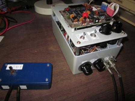
The first prototype was hand-wired and packaged into a (gray) box, as shown below, with a separate (blue) box for the test fixture.
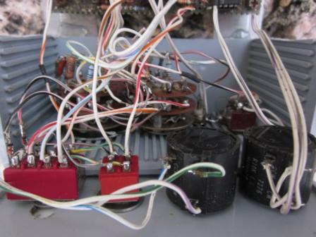
The DVM board was moved to the top of the plastic box cover to make it more accessible for prototype probing. Even this was not convenient enough, and the box was cut apart and repackaged on metal rails, as shown below.
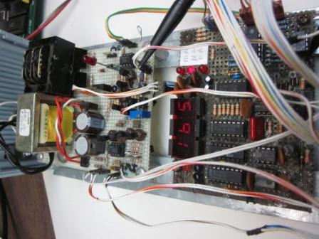
The amplifier board with power supply is in the rear (left) and the DVM board was placed next (right). In front of the DVM board are the front-panel switches and ten-turn pots. The view below is at the front of the instrument, looking down behind the front-panel.
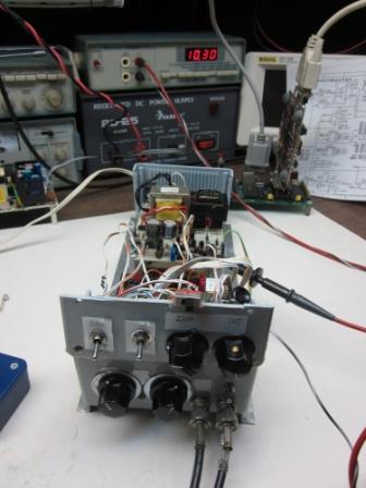
From the front, it looks like this (below). The LED display is inside the open structure and can be easily viewed from above. The circuit-board version will have everything on a single board that sets on a benchtop.
At the same time as etched circuit-board (ECB) layout occurs, the front-panel will be designed in CorelDraw as an overlay of the board. Meanwhile, the prototype has a stenciled front-panel nomenclature - adequate but not highly appealing. The CAD front-panel will be industry-grade.
Input-port voltage, current control, a 10-turn pot with a bipolar 10 V fs output voltage range and fs decade current ranges from 100 nA to 100 mA.
An input voltage, current (V, I) mode switch.
Output-port voltage control, another 10-turn pot with a fs range of 0 V to 35 V. An output polarity switch selects polarity of voltage (and current).
DVM display selection switches: V or I and INP or OUT for all four combinations of input and output port voltages and currents
Input current range switch: 7 decade ranges from 100 nA fs to 100 mA fs
Output current range switch: 7 decade ranges from 100 nA fs to 100 mA fs - same as the input port
INP-port output BNC
OUT-port output BNC
DVM display: 3.3 digit (2000 count + sign = 4000 count) LEDs. Additionally, to the right of the numerical display are three units LEDs for nA, mA, and mA. Voltage units are in V and no LED is lit for voltage measurements.
The TPA202 has a high-side current sense circuit (IISN) for the input port and a low-side circuit (OISN) for the output port. That is, the IISN is in series with the + output terminal of the INP port and the OISN is in series with the – terminal of the OUT port. The INP output BNC outer conductor is grounded, but the OUT-port amplifier BNC is floating slightly from ground by the voltage drop across the OISN circuit. Because the OISN is in series with the – terminal, a floating supply (actually, two of them: +20V and +40 V) is required for the OUT-port amplifier. The IVDR is 10 V fs and is within the range of op-amps operated from ±12 V supplies. Consequently, the high-side IISN circuit is low enough in voltage to be implemented without voltage translation.
The OUT-port amplifier OISN circuit is returned to the
amplifier ground through the output polarity switch. This switch swaps the
amplifier output terminals and consequently the OUT-port circuits must have a
floating supply. As a result of this configuration of port amplifiers, the
common (COM) terminal for the device under test (three-terminal transistor) is
floating relative to system (and INP-port) ground. It is away from ground only
by the sense-resistor voltage drop within OISN of about 0.1 V fs.
![]()
The TPA202 Manual is available to Innovatia Assistants; request a copy. It will be emailed to your requesting email address.
![]()
![]()
![]()